Semiconductors
Definition
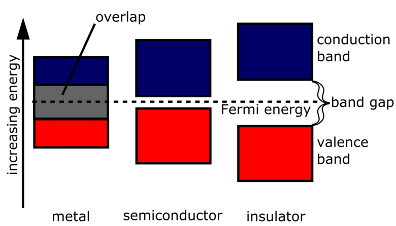
A semiconductor is a material which has a small band gap between its valence band and conduction band. Semiconductors have a conductivity between that of insulators and conductive metals.
The properties of semiconductors can be explained by energy bands - the energy levels for a crystal or lattice structure, created by the many energy levels of the atoms in the lattice being put together.
Valence Band
The valence band is the highest energy band occupied by electrons at absolute zero. Electrons in this band require the least energy to bring up to the conduction band.
Conduction Band
The conduction band is the lowest energy band in which electrons are delocalised - meaning that they can move freely between atoms in the material. Electrons being present in the conduction band of a material allows it to conduct electricity.
Band Gap
The gap between a valence band and conduction band is called the band gap. The larger the band gap is, the more energy is required for electrons to jump across it between the valence and conduction bands.
Insulators have a large band gap, and require a lot of energy for the electrons to jump from the valence band to the conduction band - which is what makes the material insulative. Conductors, on the other hand, have no band gap, as their valence and conduction bands are overlapping.
Doping
A pure semiconductor, such as a pure silicon lattice, is known as an intrinsic semiconductor. Impurities are often added to intrinsic semiconductors to increase or decrease the number of electrons in the material. This is known as doping, and it makes the semiconductor more conductive, as well as giving it other unique properties.
A semiconductor can be doped by diffusing the impurities as a gas into the liquid semiconductor as it is crystallising, which integrates the impurities into the resultant lattice structure. Silicon is usually doped with a ratio of one impurity atom to every million silicon atoms.
It is important to note that p-type and n-type semiconductors, despite having more or less electrons than the intrinsic semiconductor counterpart, are not positively or negatively charged! The change in the number of protons in the nuclei of the impurity balance out the difference in electron count, so the material as a whole remains neutral in charge.
N-Type Semiconductors
If an element with more electrons in its outer shell is added to an intrinsic semiconductor, an n-type semiconductor is formed. This results in an excess of electrons in the conduction band, which is what increases the conductivity of the material.
P-Type Semiconductors
If the impurity added to an intrinsic semiconductor instead has less electrons, then the result is a p-type semiconductor. The deficiency of electrons in the material results in nearby electrons wanting to fill the empty spaces in which electrons should be present (also known as holes), which is what increases the conductivity of the material.
P-N Junctions
When two adjacent parts of an intrinsic semiconductor are doped with p-type and n-type impurities, a p-n junction is formed as a result. The excess delocalised electrons in the n-type side of the junction want to move to the p-type side where there is a deficiency of electrons, with the resulting movement of electrons being known as electron diffusion. This results in negative ions being formed on the p-type side, and positive ions being formed on the n-type side, in a region known as the depletion region or depletion layer.
